The exponential growth of Artificial Intelligence (AI), Machine Learning (ML), and High-Performance Computing (HPC) has triggered an unprecedented demand for data throughput. Modern AI models, from large language models (LLMs) to complex genomic simulations, are not just demanding more computational power; they are demanding an entirely new level of interconnectivity. The data itself—the constant, massive flow of information between processors, memory, and networking gear—has become the primary bottleneck.
For decades, the data center industry has focused on improving processing speed (measured in FLOPS). However, as compute power continues to climb, the limiting factor is shifting from the speed of the chip itself to the speed and efficiency of the links connecting the chips. This realization has placed the spotlight squarely on optical interconnects.
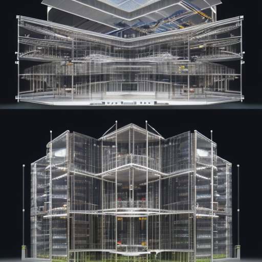
Enter Co-Packaged Optics (CPO). CPO represents a fundamental architectural shift, moving the optical engine—the components responsible for converting electrical signals into light and vice versa—from bulky, external modules onto the same substrate as the processing chip itself. This integration is not merely an incremental improvement; it is a paradigm shift that is making the next generation of AI supercomputers possible.
The Data Center Interconnect Bottleneck: Why Traditional Optics Fail AI
To understand the revolution brought by CPO, one must first grasp the limitations of the current state-of-the-art interconnects. Historically, data center architectures relied on a tiered approach: the processor (GPU/CPU) communicates with memory, and then that data is transmitted off-chip to networking modules (like transceivers) which, in turn, send it over optical cables.
This traditional "chip-to-module-to-cable" pathway introduces several critical inefficiencies:
- Power Consumption: The process of converting electrical signals to light, and then back again, at multiple physical interfaces is inherently power-intensive. Each conversion point adds significant electrical overhead, generating heat that must be managed. In massive AI clusters, where power efficiency is paramount, this overhead quickly becomes prohibitive.
- Signal Integrity and Latency: Every physical interface adds resistance, capacitance, and signal loss. These cumulative effects degrade signal integrity and introduce measurable latency. In AI applications, where milliseconds matter, this accumulated latency can cripple performance.
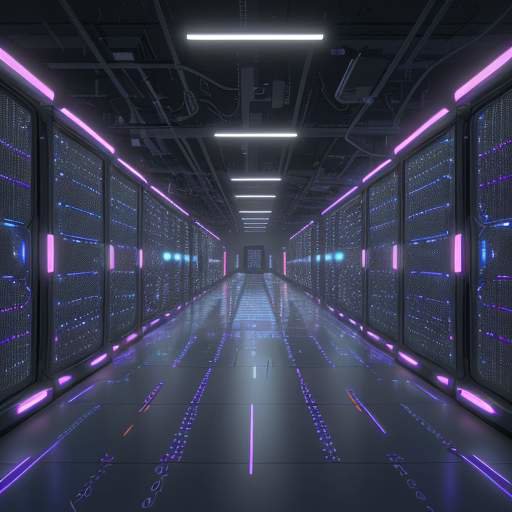
- Physical Space and Density: The external optical modules (transceivers) are bulky, requiring significant physical space and complex cooling solutions on the networking side of the rack. As compute density increases, the sheer volume of these components becomes a major limiting factor.
The fundamental problem is that the electrical signal must travel a long distance off the chip, undergo multiple conversions, and then travel back to the optical engine, all before it can be transmitted over a fiber cable. Co-Packaged Optics solves this by eliminating the long, power-hungry electrical pathways.
Understanding Co-Packaged Optics (CPO)
Co-Packaged Optics is, simply put, the physical integration of the optical components directly onto the same package substrate as the high-speed electronic processing chip. Instead of sending high-speed electrical signals from the chip’s edge out to a separate optical module, CPO allows the signal to travel a mere few millimeters to the integrated laser and modulator array.
This integration is revolutionary because it fundamentally changes the power budget equation. By minimizing the distance the signal must travel electrically, CPO dramatically reduces the required electrical power for the transmission link.
The physical implementation involves advanced packaging techniques, often utilizing silicon interposers or specialized silicon photonics wafers. These wafers house the lasers, modulators, and detectors, allowing them to be mounted in close proximity to the high-speed I/O (Input/Output) pads of the GPU or CPU.
The core benefits of this integration are threefold:
- Power Efficiency: By shortening the electrical path, the power consumed per bit transmitted drops dramatically. This is arguably the single most important factor enabling large-scale AI deployment.
- Density: Integrating the optics shrinks the physical footprint of the interconnect, allowing data center operators to pack far more compute power and networking capability into the same rack space.
- Speed and Bandwidth: The ability to manage signal integrity over extremely short, controlled paths allows for much higher signaling speeds and aggregate bandwidth capacity than was previously possible.
The Enabling Technology: Silicon Photonics
If CPO is the architectural goal, Silicon Photonics (SiPh) is the primary enabling technology. Silicon photonics refers to the integration of optical components—like waveguides, modulators, and detectors—onto a silicon chip.
Traditionally, optical components were housed in bulky, discrete packages using materials like Indium Phosphide (InP). While InP is excellent for generating light, it is difficult and costly to integrate with the mature, high-density CMOS fabrication processes used for CPUs and GPUs.
Silicon, on the other hand, is the backbone of the entire digital electronics industry. By developing specialized processes, researchers and engineers have found ways to generate, manipulate, and detect light using silicon itself.
The SiPh approach leverages the mature, cost-effective, and scalable manufacturing ecosystem of silicon wafer fabrication. This allows the entire optical engine—from the light source (laser) to the signal shaping (modulator)—to be fabricated using the same processes that create the processor itself.
The key components enabled by SiPh that make CPO possible include:
- Silicon Waveguides: Microscopic channels etched into the silicon that guide the light signal with minimal loss.
- Modulators: Devices that rapidly change the intensity of the light signal (turning it on and off at extremely high frequencies) to encode data.
- Integrated Lasers: Miniaturized light sources that are fabricated directly onto the silicon platform, eliminating the need for external, bulky laser sources.
This synergy—CPO leveraging SiPh—is what makes the entire concept economically viable and technically feasible for mass deployment in data centers.
Impact on AI and HPC: The Performance Multiplier
The connection between CPO/SiPh and the AI era is direct and profound. AI workloads, particularly those involving massive matrix multiplications (the core operation of neural networks), are characterized by two things: enormous computational density and immense data movement.
Current limitations mean that the data movement itself consumes a significant portion of the total power budget, sometimes exceeding the power needed for the actual computation. CPO addresses this by making the data movement hyper-efficient.
1. Solving the Power Wall
For AI supercomputers, the power budget is the ultimate constraint. By reducing the power consumed by the interconnects, CPO effectively increases the usable compute power within a given power envelope. This means data center operators can fit more processing power into the same physical space while staying within the cooling capacity of the facility.
2. Enabling Scale and Density
AI models are growing exponentially in size (e.g., moving from billions to trillions of parameters). To train these models, thousands of GPUs must communicate synchronously and constantly. CPO allows for much higher density of high-bandwidth connections on a single board. Instead of having a few high-power, external links, a single CPO-equipped accelerator can support dozens of ultra-high-speed, low-power links, facilitating true massive-scale parallel processing.
3. Reducing Latency for Real-Time AI
Many AI applications—such as autonomous vehicles, real-time medical diagnostics, and financial trading—require near-instantaneous processing. High latency is a killer in these fields. By minimizing the physical distance and the number of signal conversions, CPO drastically reduces the end-to-end latency, allowing AI systems to operate closer to the speed of thought.
Challenges and the Road Ahead
While the promise of CPO is immense, the technology is still maturing and faces several significant hurdles before it becomes universally adopted:
1. Thermal Management
Integrating complex optical components directly onto a high-power processor package generates a unique and challenging thermal profile. The heat must be managed at a much finer granularity than traditional cooling systems, requiring advanced liquid cooling solutions and sophisticated thermal modeling.
2. Standardization and Ecosystem Adoption
The industry is composed of diverse players (chip designers, optical component manufacturers, packaging specialists, and data center operators). Achieving industry-wide standardization for CPO interfaces, packaging, and testing protocols is critical. The industry is currently undergoing a massive, coordinated effort to establish these standards.
3. Manufacturing Complexity and Cost
The fabrication process for CPO is orders of magnitude more complex than standard chip packaging. It requires integrating disparate technologies (CMOS, photonics, and advanced packaging materials) onto a single substrate, which drives up initial manufacturing costs and requires highly specialized expertise.
Despite these challenges, the economic incentive driven by AI demand is proving to be the most powerful catalyst. The performance gains and power savings offered by CPO are simply too valuable for the industry to ignore.
Conclusion: The Future is Integrated Light
Co-Packaged Optics, powered by the breakthrough capabilities of Silicon Photonics, is not just an evolution of data center interconnects; it is a foundational technological leap. It solves the fundamental physical limitations of data movement that have plagued the industry since the dawn of the digital age.
By bringing the light source and the signal processing engine directly to the edge of the processor, CPO dramatically reduces power consumption, boosts density, and minimizes latency. This trifecta of improvements is precisely what the next generation of AI supercomputers requires to scale to truly massive levels.
As the demand for computational power continues to accelerate—driving everything from personalized medicine to climate modeling—the data highway must become faster, smaller, and more efficient. Co-Packaged Optics is building that highway, paving the way for an era of artificial intelligence that is not just powerful, but fundamentally sustainable and scalable. The era of integrated light is here, and it is redefining the very architecture of the modern data center.